Home > Products > AT8583
AT8583
Part Number Description User RAM (bytes) Working temperature range (℃) Cross Reference Power supply voltage (V) Timing current (typical) Clock format Crystal CL (pF) Integrated crystal Temperature compensation Bckup power Trickle charge Alarm / Interrupt Square wave output (Hz) Clock calibration function Power down Oscillation stop detection Pin/Package
AT8583 240 -40 to +85 PCF8583 2.6~6.0 5.0 μA (3V) HH:MM:SS 12.5 1﹣A Programmable (open drain) SOP8、DIP8

Description

       AT8583 is a CMOS real-time clock / calendar chip launched by Wuhan Xinjing Technology Co., Ltd. This chip has a built-in timer including year / month / day / hour / minute / second / percent second, which plays the role of clock in the circuit. The system can set and read the current time stored in AT8583, so as to process the data accordingly (such as billing, display, recording, etc.). Not only that, the AT8583 also comes with 240 bytes of static RAM for storing configuration data. By transmitting data between the advanced I2C bus and the system serially, the AT8583 can greatly reduce the number of wiring on the circuit board compared to the scheme using a parallel bus, which is very suitable for complex systems. AT8583 also has the function of a 6-bit BCD code event counter.

   AT8583 currently offers three packages: DIP-8, SOP-8 and TSSOP-8. It can be used in mobile phone communication products, portable instruments, telecommunications billing, time attendance, computer motherboards, microcomputer peripherals and so on. Electronics.

Device characteristics

  • Wide operating voltage range 2.6 ~ 6V

  • RAM data holding power supply voltage 1 ~ 6V

  • 50μA maximum operating current when the bus is idle

  • 4-year calendar clock, selectable 24-hour or 12-hour format, external oscillator can input 32.768KHz or 50Hz signal as time base

  • Programmable alarm, timing and interrupt functions

  • Fully compatible with Philips PCF8583

Pin arrangement and description


Pin name

Pin number

Description

OSCI

1

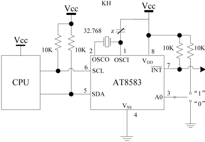
Connect a pin of 32.768KHz crystal, frequency trimming capacitor should be added to this pin; external oscillator signal can also be introduced

OSCO

2

Connect another pin of 32.768KHz crystal. OSCI pin should be left floating when external oscillator signal is introduced

A0

3

Hardware address selection pin, one I2C bus can be connected to two AT8583-as long as the A0 pin levels of the latter are different from each other

VSS

4

Ground

SDA

5

Serial data I / O (open-drain)

SCL

6

Serial clock input (open-drain)

INT

7

Interrupt output (open-drain)

VDD

8

Positive power

Typical application circuit

微信图片_20200615145824.png


Support:万广互联 Copyright © 2008-2020 Analog Tek Technology Co, Ltd 鄂ICP备20005446号-1